
6-layer high-frequency PCBs are widely used in the communications industry
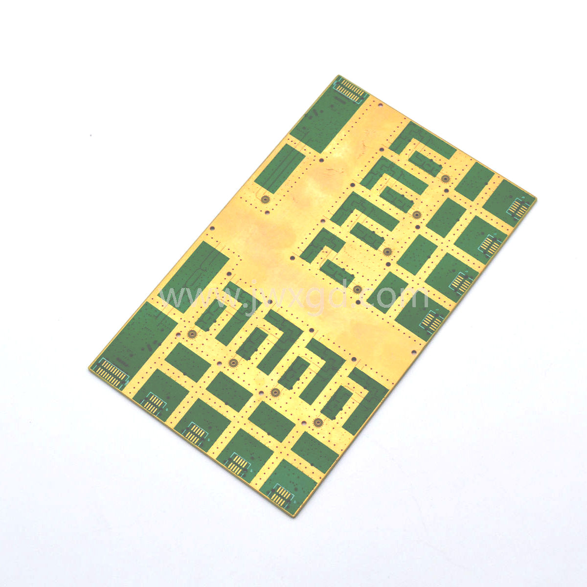
Layer: 6L ENIG Plated Through-Hole High-Frequency PCB
Material: RO4350
Finished Thickness: 1.6 mm ± 0.1 mm
Minimum Via Hole Size: 0.3 mm
Minimum Line Width / Spacing: 125 μm / 100 μm
Minimum Pad Size: 0.3 mm
Solder Mask & Legend Color: Photoimageable Green / White
Gold Plating Thickness: 0.05 μm
Special Process: Fabrication with high-speed material technology