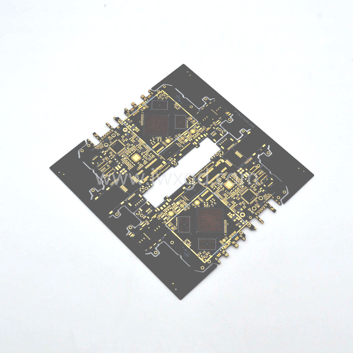

10-Layer 1-Step HDI PCB is engineered for high-performance industrial control applications.
Layer: 10L, 1-Step HDI PCB
Material: Shengyi S1000-2M
Finished Thickness: 1.2 mm ± 0.1 mm
Minimum Via Hole Size: Laser Via: 0.1 mm; Mechanical Via: 0.2 mm
Minimum Line Width / Spacing: 75 μm / 75 μm
Minimum Pad Size: 0.2 mm
Solder Mask & Legend Color: Matte Black / White
Surface Finish: OSP + ENIG 0.05 μm
Special Process: Multiple lamination, resin via plugging, via filling & plating, dual surface finishing